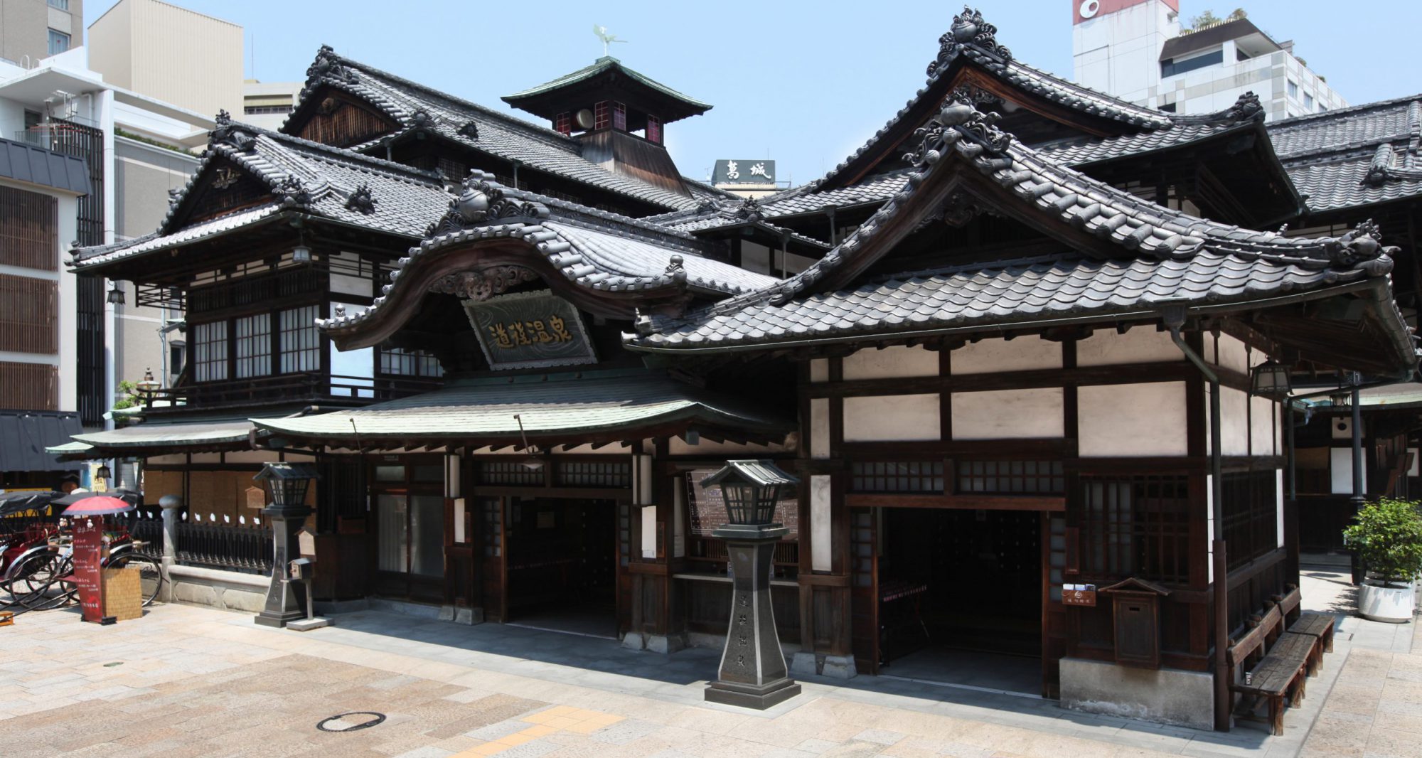
Keynote 1 (10:30–11:30, November 23)
Machine Learning for Serving Test Data Analytics
Speaker: Prof. Li.-C Wang (University of California, Santa Barbara)
Abstract: Applying machine learning in test data analytics has been researched for many years. In the field of semiconductor test, data seems to be abundant and opportunities to take advantage of modern ML technologies seem to be many. Nonetheless, often in practice when a practitioner is asked to build and deploy a ML solution, it can still be a daunting task, demanding much R&D effort with no clear sight of ending success. The situation is quite different for other ML applications, such as those involving computer vision and language understanding, where tremendous growth has been observed in the past few years. In view of this gap, this talk discusses promises and barriers for realizing a ML solution in test data analytics. To overcome the potential barriers, this talks advocates taking a top-down approach that starts with questions at the operation intelligence level and then sketches a system to provide a specification for the required machine learning services. It is after such a system view is specified can one better understands what ML components are needed and whether they can be realized with the current ML technologies and the available data. Practical examples and experiment results are used to illustrate the top-down approach and its key considerations.
Biography: Li-C. Wang, is a professor of the ECE department and the Chair of Computer Engineering program at University of California, Santa Barbara. He received PhD in 1996 from University of Texas at Austin, and was previously with Motorola PowerPC Design Center until 2000. Since 2003, his research has been focusing on machine learning specifically for applications in EDA and Test. He received in total 10 Best and Honorable Mentioned Paper Awards from major conferences, including more recently from ITC 2014, ITC 2019, VLSI DAT 2019 and VTS 2016. He is the recipient of the 2010 Technical Excellence Award from Semiconductor Research Corporation, and the recipient of the 2017 IEEE TTTC Bob Madge Innovation Award. He is a fellow of IEEE. He was the General Chair of the International Test Conference (ITC) in 2017 and 2018. With that role, he participated in founding the ITC Asia conference and served as the General co-Chair for its first event. https://iea.ece.ucsb.edu/
Keynote 2 (11:00–12:00, November 24)
Supercomputer Fugaku System – Technologies to Promise its Quality and Reliability
Speaker: Dr. Takahide Yoshikawa (Fujitsu)
Abstract: The supercomputer Fugaku, which achieved the world’s fastest prize in 2020, is a huge and extremely complex system consisting of more than 150,000 CPUs and 100,000 optical cables with a total length of more than 900km. In order to assure the quality of this system within the limited development period, it is indispensable to find bugs and issues at the earliest stage. Therefore, appropriate verification and test schemes should be applied to each development stage, from requirements definition to manufacturing. In this presentation, I will give an overview of the Fugaku system and then introduce various kinds of technologies, such as pre-silicon verification (simulation and formal), tests (DFT, ATPG), post-silicon validation (test fixture and test generator), and manufacturing test. These schemes ensured the Fugaku system’s quality and reliability as early as possible.
Biography: Takahide Yoshikawa is a Project Manager of Advanced Computing Project, Fujitsu Laboratories at Fujitsu Ltd. He received his B.E., M.E., and Ph.D. degrees from the University of Tokyo in 1994, 1996, 2002, respectively, and also, he is a Senior Member of IEEE. He has been involved in various kinds of server systems projects, such as the K computer and Fugaku. In the K computer project, he proposed and implemented the whole verification, validation, and test system of its interconnect, Tofu. In Fugaku, he led the verification and validation of the CPU. Currently, he is tackling research on the architecture of the future high-performance system.
Keynote 3 (12:30–13:30, November 24)
Optically Efficient III-V Compound Semiconductor Nanowires on Si
Speaker: Prof. Fumitaro Ishikawa (Ehime University)
Abstract: The integration of III-V semiconductor nanowires on Si substrates can introduce superior optical functions into developed Si technology. For its application requiring large output like energy conversions, e. g., photovoltaics or photo-electrochemistry, the volume and electron-photon conversion efficiency is a vital issue. We grow III-V GaAs-related nanowires (NWs) ensembles using self-catalyzed Ga induced vapor-liquid-solid growth, which show bright and homogeneous room temperature photoluminescence over 2-inch Si(111) substrate. Those are grown without specific pre-treatment such as patterning, film deposition, nor etching on the Si substrate, promising to cost-effective productions. We observe dark surface at the area having dense NWs, where NWs absorb the incident light. The sample shows homogeneous NWs distributions over the substrate surface, showing the NWs typically having their length and diameter of 5 µm and 300 nm, respectively, with their density of 5×107 cm-2. Our recently proposed passivation with outermost AlGaOx native oxide shell provides efficient GaAs inner core luminescence efficiency at room temperature. Then the sample shows bright photoluminescence having their intensity comparable or stronger than commercially available p-type GaAs substrate with homogeneous peak wavelength distributions. We can extend the NWs functions by controlling crystal structure, introducing nitrogen for its application to lasers, bismuth for promising quantum structure, and oxidation for its application to white light source. These results would open up the prospect for large volume optical energy conversion on Si platform.
Biography: Fumitaro Ishikawa is an associate professor of Graduate School of Science and Engineering at Ehime University, Japan. He received his doctoral degree from Hokkaido University in 2004. After serving as Visiting Scientist at Paul Drude Institute, Berlin, he was appointed to an assistant professor at Osaka University in 2007, and became his current position in 2013. His research interests are in the area of crystal growth of compound semiconductor nanostructures with molecular beam epitaxy and functional electronic materials.
